
60 Gb/s 1:4 Demultiplexer in 22-nm FD-SOI Technology
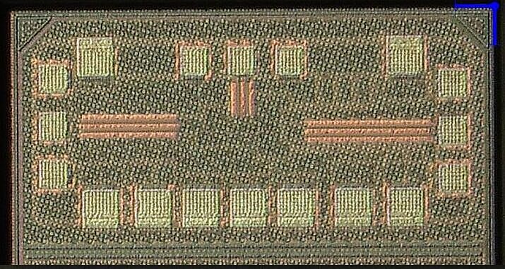
This chip implements a 1:4 single-ended binary-tree demultiplexer designed for ultra-high-speed serial data systems. It converts a high-rate serial input stream into four parallel outputs, enabling subsequent digital circuits to operate at lower clock frequencies. The architecture uses a binary-tree structure composed of true single-phase clock (TSPC) flip-flops, latches, and a frequency divider, all implemented using compact gated-inverter blocks. This design approach enables high-speed operation while keeping the circuit area extremely small. The demultiplexer supports input data rates from 1.6 Gb/s up to 60 Gb/s, providing a wide operational range for different applications. The circuit can operate with supply voltages between 0.6 V and 1.2 V, allowing flexible trade-offs between performance and power consumption. Fabricated in 22-nm FD-SOI CMOS technology, the chip occupies only 0.033 mm². Its power consumption is mainly dynamic and naturally scales with the input data rate due to the inverter-based architecture.
References
B. Sadiye, M. Iftekhar, W. Mueller and J. C. Scheytt, "60-Gb/s 1:4 Demultiplexer in 22-nm FD-SOI Technology Using TSPC Logic: A Circuit-to-System-Level Analysis and Design," in IEEE Transactions on Very Large Scale Integration (VLSI) Systems, vol. 34, no. 2, pp. 366-378, Feb. 2026, doi: 10.1109/TVLSI.2025.3625787.